Market Snapshot
Key Takeaways
Market Overview & Analysis
Report Summary
The automotive chiplet market comprises the value of chiplet-based semiconductor compute content installed in light vehicles worldwide, where a chiplet is a small modular die performing a specialised function that is combined with other dies in a single package to build a central vehicle computer in place of a monolithic system-on-chip. This study segments the market by packaging technology, chiplet function, application domain, interconnect standard, vehicle class and region, with a 2025 base year, historical coverage from 2021 to 2025, and forecasts to 2030.
Sizing method requires explicit statement because no manufacturer reports chiplet-based automotive silicon separately. The market is computed as the number of vehicles shipping chiplet-based compute architecture multiplied by chiplet content value per vehicle, both stated so that either can be substituted and the result recomputed. That figure was cross-checked top-down: global light vehicle production near 90.0 million units at roughly USD 730 of semiconductor content per vehicle gives about USD 65.7 billion of automotive semiconductors, of which central compute and high-performance system-on-chips represent roughly 15%, and chiplet-based architectures about 5.6% of that in 2025.
The distinction between the automotive chiplet market and the wider chiplet market matters commercially. Published chiplet market figures spanning tens of billions of dollars refer overwhelmingly to data centre and enterprise computing, where the architecture reached volume years earlier. Automotive is a small and late sub-segment of that total, constrained by qualification cycles, functional safety requirements and temperature range specifications that data centre parts do not face. Readers comparing the two should expect roughly two orders of magnitude difference.
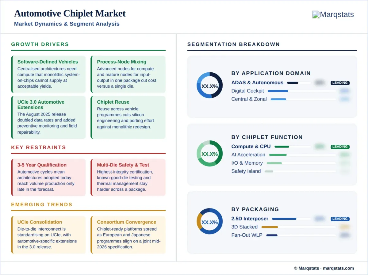
Chiplets solve a problem specific to software-defined vehicles. Centralised electrical and electronic architectures require far more compute than distributed control units, yet monolithic system-on-chips large enough to supply it suffer poor yields and long development cycles. Chiplets allow processing, artificial intelligence acceleration, input-output and safety functions to be manufactured on different process nodes, combined in one package, and reconfigured between vehicle programmes without redesigning the whole device.
Market Dynamics
Key Drivers
- Software-defined vehicle architectures demand centralised compute that monolithic system-on-chips cannot supply economically at acceptable yields.
- Mixing process nodes within one package allows advanced nodes for compute and mature nodes for input-output, reducing cost against a single-node monolithic device.
- The UCIe 3.0 specification released in August 2025 added automotive-specific features including preventive monitoring, run-time link-health testability and field repairability.
- A European research institute's automotive chiplet programme has grown to twenty-two partners spanning manufacturers, suppliers, foundries and design tool providers.
- Chiplet reuse across vehicle programmes reduces silicon engineering resource requirements and porting effort materially against monolithic redesign.
Key Restraints
- Automotive qualification cycles run three to five years, so architectures adopted today reach volume production only toward the end of this forecast.
- Functional safety certification to the highest automotive integrity level is more complex across a multi-die package than a single monolithic device.
- Known-good-die testing and thermal management in a package spanning multiple suppliers remain unresolved cost and yield problems.
- Standardisation is incomplete, with a joint public specification between the principal European and Japanese initiatives targeted for the middle of 2026 rather than delivered.
Key Trends
- Interconnect standardisation is consolidating around UCIe, with automotive-specific extensions added in the 3.0 release.
- Compute subsystem vendors are shipping chiplet-ready automotive platforms with standardised die-to-die connectivity for third-party accelerators.
- Tier-one suppliers and semiconductor firms are forming direct chiplet development partnerships outside conventional supply relationships.
- Regional standardisation efforts are converging, with a joint specification between European and Japanese programmes targeted for mid-2026.
Market Segmentation
Two-and-a-half-dimensional packaging using silicon interposers or organic substrates accounts for the largest share of automotive chiplet deployment, placing multiple dies side by side on a shared interconnect layer. The approach is the most mature, carries the most thoroughly understood thermal characteristics for automotive temperature ranges, and is where existing qualification experience sits. Bridge-based variants that embed a small silicon bridge in the substrate rather than a full interposer reduce cost and are gaining share in cost-sensitive programmes.
Three-dimensional stacking places dies vertically with through-silicon vias, achieving the highest interconnect density and shortest signal paths. Thermal dissipation is the binding constraint in automotive applications, where ambient temperatures far exceed data centre conditions and forced cooling is limited. Fan-out wafer-level packaging grows fastest of any approach, eliminating the interposer entirely and offering the lowest cost path to volume, which makes it the likely mid-market architecture as chiplets move beyond premium programmes.
Central processing chiplets account for the largest share of automotive chiplet value, supplying the general-purpose compute that runs vehicle operating systems and application software. Artificial intelligence accelerator chiplets grow fastest of any function, driven by perception and planning workloads in advanced driver assistance and autonomous systems, and they are the function most frequently sourced from a different supplier than the main compute die, which is precisely the modularity chiplets enable.
Input-output chiplets handle vehicle network connectivity, sensor interfaces and external communication, and are typically manufactured on mature process nodes where advanced geometry brings no benefit. That node mixing is one of the strongest economic arguments for chiplet architectures. Memory chiplets provide high-bandwidth local storage adjacent to compute. Safety island chiplets run the certified monitoring functions required for the highest automotive integrity levels, isolated from application processing.
Advanced driver assistance and autonomous driving is the largest application domain for automotive chiplets and the primary reason the architecture is being adopted, since perception and planning workloads demand compute at levels monolithic automotive system-on-chips struggle to deliver economically. The domain also carries the strictest functional safety requirements, which is why safety island chiplets and certified monitoring architectures are integral to designs targeting this application rather than optional additions.
Digital cockpit and infotainment applications consolidate instrument clusters, head units, passenger displays and voice assistants onto shared silicon, and they were among the earliest automotive workloads to justify high-performance compute. Central compute and zonal controller architectures represent the fastest-growing application, combining previously separate domains onto a single platform, and they are where chiplet modularity delivers the clearest benefit because the workload mix varies between vehicle programmes.
The Universal Chiplet Interconnect Express standard has become the dominant open die-to-die interconnect for automotive chiplet designs. The 3.0 specification released in August 2025 doubled peak data rates to 48 and 64 gigatransfers per second from 32 in the prior release, and added explicit automotive-segment enhancements including preventive monitoring, run-time link-health testability and field repairability, alongside runtime recalibration and early firmware download through the management transport protocol. Those additions address automotive requirements that general-purpose interconnect standards did not.
Proprietary die-to-die interfaces remain in use where a single vendor supplies all dies in a package and interoperability carries no value, and they can be optimised more aggressively than a general standard permits. Alternative open standards including bunch-of-wires interfaces occupy a smaller position, favoured in cost-sensitive designs where simpler physical layers reduce implementation overhead. Proprietary share declines as multi-vendor packages become the norm and as the commercial case for interoperability strengthens.
Premium and luxury vehicles account for the substantial majority of chiplet-based compute deployment in 2025, because they carry the most capable compute platforms and absorb the highest silicon content per vehicle. Content value per vehicle of about USD 833 in 2025 reflects this concentration. The segment functions as the qualification and validation ground for architectures that subsequently migrate downmarket, which is the standard automotive electronics adoption pattern.
Mid-market vehicles account for a small share of 2025 deployment and the overwhelming majority of forecast growth, and their entry is what drives content value per vehicle down to about USD 539 by 2030 while unit volumes rise thirteen-fold. Commercial vehicles adopt more slowly, with longer development cycles and different compute priorities weighted toward fleet telematics and driver monitoring rather than autonomous capability, though the modularity argument applies equally.
Asia-Pacific accounts for the largest share of automotive chiplet deployment, reflecting both regional vehicle production volumes and the concentration of advanced packaging capacity in Taiwan, South Korea and China. Japan hosts the most structured national initiative, a research consortium founded in December 2023 by twelve companies spanning vehicle manufacturers, tier-one suppliers, semiconductor firms and design tool providers, targeting in-vehicle chiplet technology by 2028 and mass-production installation from 2030.
North America hosts the principal compute silicon designers supplying automotive chiplet platforms and the interconnect standards body, though vehicle assembly volumes are lower than Asia-Pacific. Europe hosts the principal collaborative research programme, run by a Belgian research institute and now spanning twenty-two partners including German and American vehicle manufacturers, tier-one suppliers, foundries and design tool vendors. Rest of World deployment is negligible, since chiplet adoption follows advanced vehicle programme development rather than assembly location.
By Geography
Asia-Pacific
Asia-Pacific leads automotive chiplet deployment and hosts the majority of the advanced packaging capacity the architecture depends on. Japan's national research consortium, founded in December 2023 by twelve companies including major vehicle manufacturers, a major tier-one supplier, a manufacturer joint venture and semiconductor and design tool firms, has the clearest published roadmap in the industry: in-vehicle chiplet technology established by 2028 and chiplet-based system-on-chips installed in mass-produced vehicles from 2030, supported by nationally funded research adopted in March 2024.
North America
North America hosts the compute silicon designers whose automotive platforms are driving chiplet adoption, and the consortium responsible for the dominant open die-to-die interconnect standard. Vehicle programme development for advanced driver assistance and autonomous systems is concentrated here, and it is programme development rather than assembly volume that determines chiplet demand. Several electric vehicle manufacturers headquartered in the region are among the earliest adopters of centralised compute architectures suited to chiplet implementation.
Europe
Europe hosts the principal collaborative automotive chiplet research programme, run by a Belgian research institute, which announced its first partners in October 2024 and has since grown to twenty-two participants spanning vehicle manufacturers, tier-one suppliers, foundries, packaging houses and electronic design automation vendors. In December 2025 the institute launched a strategic alignment initiative with the Japanese consortium on automotive chiplet standards, with a joint public specification targeted for the middle of 2026, a target rather than a completed deliverable.
Rest of World
Rest of World deployment is negligible and expected to remain so across the forecast. Chiplet adoption follows advanced vehicle programme development, functional safety engineering capability and access to advanced packaging capacity, none of which is present at scale outside the three principal regions. Vehicles assembled in other markets increasingly incorporate compute platforms designed elsewhere, so regional deployment attribution follows programme origin rather than assembly location.

How Competition Is Evolving
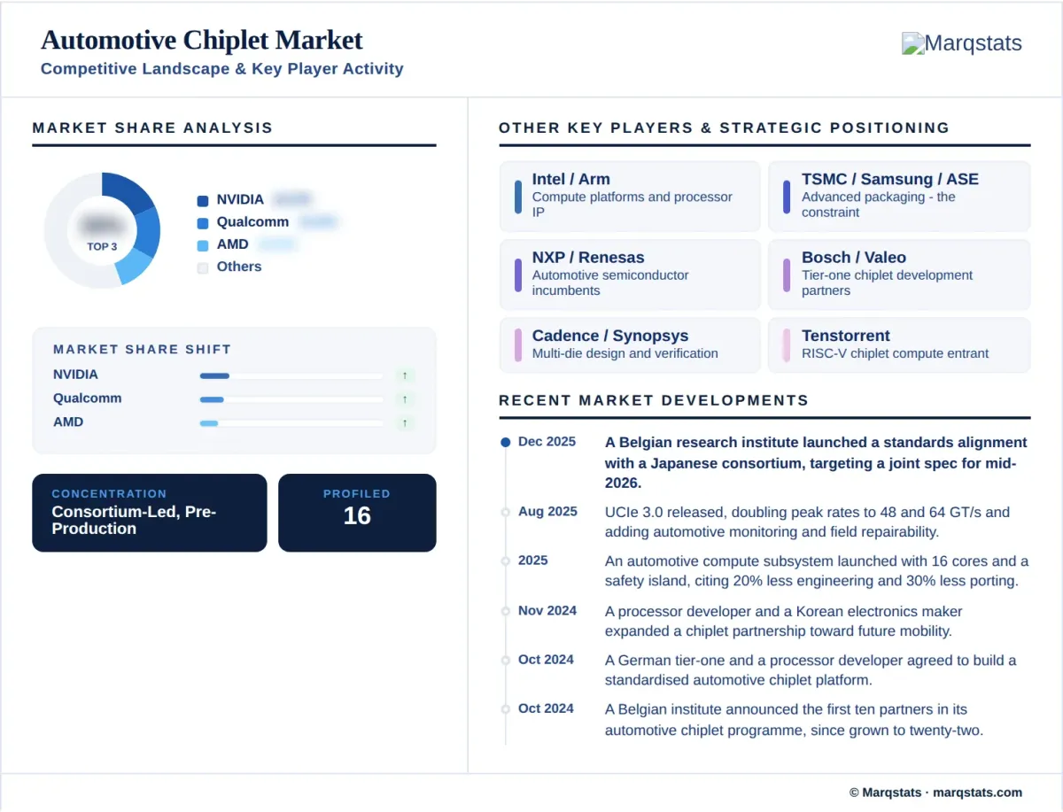
The automotive chiplet market is being assembled by consortium rather than contested by incumbents, which is unusual and reflects its pre-production stage. Two collaborative programmes dominate: a Belgian research institute's automotive chiplet programme, which announced its first ten partners in October 2024 and has grown to twenty-two, and a Japanese research consortium founded in December 2023 by twelve companies. In December 2025 the two launched a strategic alignment initiative on standards, with a joint public specification targeted for mid-2026.
Compute silicon designers hold the strongest commercial positions. Suppliers of automotive compute platforms have moved to chiplet-ready architectures with standardised die-to-die connectivity permitting third-party graphics and artificial intelligence accelerators, and one automotive compute subsystem launched in 2025 combines sixteen application processor cores with a dedicated safety island, citing up to 20% lower silicon engineering resource requirements and 30% less porting effort while supporting the highest automotive functional safety and cybersecurity standards.
Tier-one suppliers and semiconductor firms have begun forming direct development partnerships outside conventional supply relationships. A German tier-one supplier and a North American reduced-instruction-set processor developer agreed in October 2024 to develop a standardised automotive chiplet platform, and the same processor developer had earlier partnered with a Korean electronics manufacturer on chiplet collaboration for automotive products, expanding that partnership in November 2024 toward future mobility applications.
Foundries, packaging houses and design tool vendors occupy the enabling positions and participate in both consortia. Advanced packaging capacity is the physical constraint on the market, and it is concentrated among a small number of Taiwanese, Korean and American suppliers whose automotive allocation competes directly with far larger data centre demand. Electronic design automation vendors supply the multi-die design and verification flows without which chiplet architectures cannot be developed, and both major vendors participate in the European programme.
Companies Covered
The report profiles 16+ companies with full strategy and financials analysis, including:
Recent Market Activity
Table of Contents
Coverage & Segmentation
This report provides a comprehensive assessment of the automotive chiplet market across a 2025 base year, historical data from 2021 to 2025, and forecasts spanning 2026 to 2030. Market value covers chiplet-based semiconductor compute content installed in light vehicles, with vehicles shipping chiplet-based architecture reported as the volume metric. Segmentation covers six dimensions. The wider chiplet market, dominated by data centre and enterprise computing, is referenced for context and is roughly two orders of magnitude larger.
The scope covers adoption drivers, restraints and structural trends, with particular focus on the pre-inflection stage of the market and the 2030 mass-production milestone, interconnect standardisation under UCIe, consortium-led development, packaging technology selection, and the migration from premium to mid-market vehicle programmes. Adjacent automotive electronics context is available in the EV Repair and Maintenance Services Market report. An extended forecast to 2035 is available under customization, alongside design-win tracking on request.